Core components for energy-saving electronics.
Text: Christine Möller
Topological insulators are an entirely new class of materials boasting unique properties that make them promising candidates for energy-saving, high-performance electronics and quantum computers.
Smartphones and computers are everywhere. Making calls, chatting, watching films, taking photos, recording videos, surfing the net or using fitness, health or entertainment apps – all of these activities require huge amounts of energy. And not just to power the billions of end devices, but also to run the servers that store the steadily growing streams of data they process.
Modern electronics rely on components made of silicon. Silicon is a semiconductor with electrical properties that can be modulated by deliberately introducing other atoms into its crystal structure – a process known as doping.
However, the remaining optimization potential of silicon components is close to being exhausted. Accordingly, the search is on for new materials suited to the production of even more compact chips and transistors that are able to run on very little power while producing almost no heat. Topological insulators are a class of materials that meet these requirements, with the potential to usher in a major breakthrough in the performance and energy efficiency of present-day electronic devices.
Insulating on the inside, conductive on the outside
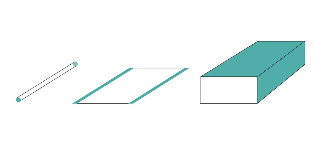
Topological insulators are distinguished by a particular feature: whereas on the inside they behave like insulators, meaning they do not conduct electricity, their edges exhibit metallic properties, making them electrically conductive. Accordingly, a three-dimensional crystal of a topological insulator only conducts electricity on its surface; currents cannot flow on the inside. Two-dimensional topological materials consisting of just a few atomic layers only conduct electricity at the edges. And in the case of a one-dimensional material – an atomically thin wire – only the charge carriers at each extremity can move.
Eliminating energy losses
Another remarkable property of these materials is that the abovementioned regions conduct current almost losslessly: resistance is minimal, so virtually no heat is generated. This effect is caused by quantum mechanical phenomena. Consequently, using these materials in electronic components has the potential to deliver unprecedented efficiency by eliminating the energy losses associated with heat generation.
Moreover, one-dimensional topological insulators could function as ideal storage units for quantum information, which would allow them to play a crucial role in quantum computers. The charge-carrying points at each end of the atomically thin wire could potentially be defined as the two components of a quantum bit – the smallest unit of information in a quantum computer.
While topological insulators could be destined for great things, they are a relatively recent discovery. It was not until the 1980s that a team of physicists led by Professor Klaus von Klitzing observed that an extremely thin two-dimensional material subjected to a very strong magnetic field at low temperatures did not behave like a true insulator as expected. Instead, it turned out to be highly conductive – at the edges. What is more, the energy losses were minimal. The discovery of this phenomenon, dubbed the quantum Hall effect, earned Klaus von Klitzing a Nobel prize in 1985.
More recently, researchers have discovered that numerous other two-dimensional and three-dimensional crystals exhibit the same peculiar properties without the need for a magnetic field. Scientists at the University of Basel are among those researching these highly promising materials.
Stacking potential
The research team led by Professor Christian Schönenberger, for instance, is searching for new topological insulators that possess particularly favorable properties for various applications. With the support of an Advanced Grant from the European Research Council (ERC), the group is investigating van der Waals heterostructures – stacks of two-dimensional crystals made up of individual atomic layers of different materials. These layers are held together by a form of attraction known as van der Waals forces. “We can now create new materials that do not occur in nature – simply by stacking two dimensional crystals in the right way. These crystals can exhibit entirely novel properties, in some cases becoming topological insulators,” explains Christian Schönenberger.
Another team led by Professor Dominik Zumbühl has developed a method allowing them to investigate the narrowly limited conductive regions of the materials. Using a technique called tunneling spectroscopy, the researchers have already succeeded in obtaining an exact “fingerprint” of these conductive regions in nanometer resolution. They predict that the method will also lend itself to highly detailed examination of topological insulators. This could help to gain even more detailed insights into the properties of these materials, and help pave the way for practical applications.
By conducting measurements on bismuth telluride, one of the first confirmed topological insulators, the group led by Professor Ernst Meyer recently succeeded in proving for the first time the theoretical assumption that resistance results in significantly lower heat generation than that caused by a comparable electrical current in conventional conductors. “Besides the low energy losses in the form of heat, we were also able to describe a novel quantum mechanism that we can use to control the resistance with a high degree of precision,” Meyer explained. “Just as a vehicle relies on resistance to start moving, accelerate or brake, it is sometimes desirable at the nanoscale, too. For potential applications, the ability to control this factor is crucial.”
There are still numerous unresolved issues for the scientific community to address before topological insulators can complement or replace present-day silicon components. In the coming years, we can expect to gain numerous new insights into this young class of materials that will bring them closer to the application stage – potentially even as components in a powerful quantum computer.
More articles in the current issue of UNI NOVA.

